
Manufacturable Optical Design & Engineering: Where Optical Performance Meets Production Reality
Many optical lens designs perform well in simulation but still fail during mass production — because ray tracing models a perfect geometry, not the shrinkage, flow stress, and tolerance stack-up that real injection molding introduces. ATRMOLD’s optical design and engineering team is headquartered in Shenzhen with a dedicated engineering facility in Dongguan, China, bridging the gap between optical design and manufacturability for every project.
With over 20 years of experience in optical lens design and injection-molded optics, our engineers review feasibility before tooling begins — at the stage where design changes are still inexpensive to make.
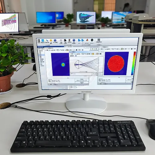
20+
Years Optical Engineering Experience
1–2 Wks
DFM Review Turnaround
≤0.001°
Angular Error Control
100+
OEM/ODM Engineering Partners
Optical Lens Design Failures We Catch Before Tooling Begins
A design that passes ray-tracing simulation is not the same as a design that survives injection molding. These three gaps account for most of the mold rework we see on projects that arrive without a manufacturability review.
Design Gap
Wall thickness that looks fine in CAD causes sink marks or warpage after molding
ROOT CAUSE:
Uniform-looking wall sections shrink unevenly once real material flow and cooling are introduced.
OUR FIX:
Wall thickness ratios are reviewed against mold-flow simulation during DFM, before any cavity is cut.
Design Gap
Tolerance stack-up that is mathematically correct still produces parts the mold cannot hold
ROOT CAUSE:
Optical tolerances assigned independently of one another, without checking what cumulative variation the mold and process can actually achieve.
OUR FIX:
Tolerance stack-up analysis is run against real mold capability data, not just the optical specification on paper.
Design Gap
Gate placement chosen for moldability introduces birefringence that ruins optical performance
ROOT CAUSE:
Gate location is often decided by the moldmaker after the optical design is finalized — too late to account for flow-induced stress in the optical path.
OUR FIX:
Gate position is evaluated jointly with optical performance requirements during the design stage, not handed off afterward.
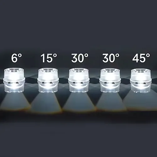
Manufacturable Optical Design for Stable Mass Production
Our optical design process integrates mold structure, injection parameters, and material behavior from the earliest design stages — not as an afterthought once tooling has already begun.
- Optical lens and imaging system design
- Ray tracing and optical simulation combined with mold-flow analysis
- Material selection across PMMA, PC, COP, and optical-grade plastics
- Design optimization linked directly to mold construction and process limits
- Long-term repeatability and yield-focused engineering
Optical Engineering Workflow: From Feasibility Review to Mass Production
We support customers from feasibility evaluation to stable mass production, integrating optical design, precision mold development, and injection molding into one framework — not three separate vendor relationships.

Requirement Review
Optical, mechanical, and production volume requirements are translated into concrete design targets — focal length, transmittance, operating temperature, mechanical load.

Design & Simulation
Ray-tracing simulation in Zemax OpticStudio with tolerance control built in from the start, not added after the geometry is finalized.

DFM & Mold Feasibility
Design for Manufacturability review validates wall thickness, gate placement, and tolerance stack-up against real mold and process limits.

Precision Mold Development
Mold construction proceeds only after design and feasibility are jointly validated — see our mold manufacturing page for tooling details.

Trial Molding & Validation
First-article samples are tested against the original optical specification — focal accuracy, transmittance, dimensional fit.

Mass Production Ramp-Up
Process parameters validated during trial are locked and monitored through full-volume ramp-up — see our injection molding page for production controls.
Resolving a 0.2mm Diameter Deviation in a Medical Optical Lens
THE PROBLEM
A U.S. medical device customer experienced production instability traced to a 0.2mm diameter deviation in a critical optical lens component.
OUR APPROACH
ATRMOLD re-evaluated the optical geometry, reallocated dimensional tolerances, and validated mold feasibility against the revised design before any tooling changes were made.
THE OUTCOME
Stable optical performance was restored. The redesigned lens has remained in continuous mass production for over five years with no recurrence of the deviation.
5+ years in continuous mass production since the redesign — zero recurrence of the original deviation.
Production-Oriented Optical Design & Precision Processing
Optical design and mold engineering are handled by the same team — eliminating the disconnect that occurs when a design house and a mold shop are two separate companies.
- Optical system design using Zemax OpticStudio, the industry-standard platform for ray tracing and tolerance analysis
- Multi-material optical design across PMMA, PC, COP, and optical glass
- 5-axis CNC machining centers with FANUC control systems, delivering ±0.0005mm repeatability
- Precision machining of aspheric and freeform optical surfaces
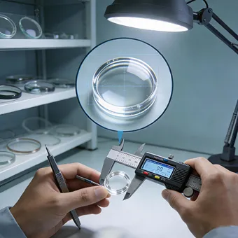
- Precision EDM equipment achieving surface finish Ra ≤0.02µm for fine optical detail and sharp internal features
Critical angular error is controlled to ≤0.001° for demanding optical systems. For context, this is the level of control that separates a sensor lens performing consistently across a 100,000-piece production run from one that drifts out of spec after the first few thousand parts.
Closed-Loop Testing & Verification Systems
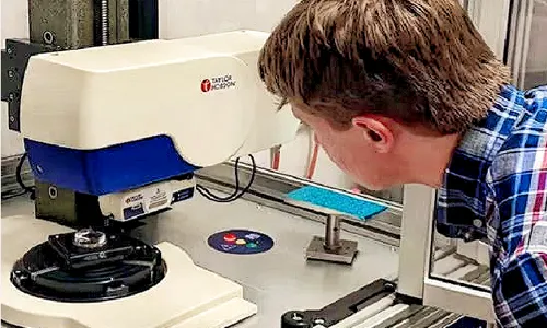
Testing is integrated into both design validation and production control to ensure batch-to-batch consistency — not applied only at final inspection.
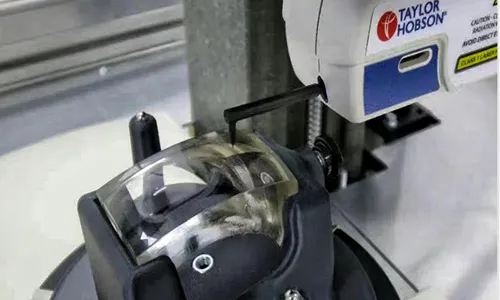
Zygo Interferometer
Surface form and wavefront accuracy verification for critical optical surfaces.
Accuracy: λ/10
Zeiss CMM
Coordinate measuring machine for dimensional accuracy across complex lens geometries.
Accuracy: ±0.0003mm
UV-Vis Spectrophotometer
Transmission validation across the optical wavelength range for every material batch.
Full visible + NIR range
Thermal Cycling Chamber
Production monitoring under simulated environmental stress before shipment approval.
-40°C to 85°C
Optical Design Solutions Engineered for Industry-Specific Requirements
VR & LED Optics
Display and illumination optics need high-transmission material paired with mirror-polished mold surfaces — any surface roughness at this scale scatters light and reduces perceived brightness or image clarity.
Protective Eyewear
Dimensional tolerance is held within ±0.02mm because frame fit and optical alignment both depend on it — a lens slightly out of tolerance can pass inspection visually but fail in actual frame assembly.
Aspheric & Freeform Lenses
Complex non-spherical geometries are engineered for low distortion using 5-axis machining and EDM — standard 3-axis tooling cannot reproduce these surface profiles to optical tolerance.
Medical Optics
Dynamic process temperature control is used to achieve production yields above 98%, because medical optical components typically cannot tolerate the rework or rejection rates acceptable in other industries.
Quality Assurance & Proven Manufacturing Capabilities
- ISO 10110 compliant optical design verification and drawing standards
- Mold inspection using Zeiss CMM and Zygo interferometry
- Production monitoring with thermal cycling from -40°C to 85°C
- Full traceability documentation through shipment approval
ISO 10110 is the international standard for specifying optical element tolerances on technical drawings. Designing to this standard from the outset reduces ambiguity between your optical specification and what our mold and molding process can actually deliver.
Related Services
Optical Design & Engineering: Frequently Asked Questions
Common questions from engineers and procurement managers about our optical design and engineering services.
Both. We develop new optical lens designs from application requirements using ray tracing and simulation in Zemax OpticStudio, and we also review and refine existing designs — particularly when a design that works in simulation is proving difficult or costly to mold at volume.
Our DFM review evaluates wall thickness, draft angles, gate location, and tolerance allocation against real mold and injection molding process limits — identifying issues such as warpage risk, sink marks, or optical distortion before any tooling is cut.
Yes, this is a common scenario. A design that passes ray-tracing simulation can still fail in production if tolerance allocation, gate location, or material behavior were not considered during the design phase. Our engineering case study above describes a similar situation — a 0.2mm deviation traced back to the original design assumptions, resolved through re-evaluation of optical geometry and tolerance allocation.
Dimensional tolerance control within ±0.02mm is standard for applications such as protective eyewear, with angular error controlled to within ≤0.001° on demanding optical systems. Specific achievable tolerances depend on lens geometry, material, and production volume — confirmed during the feasibility review stage.
Yes. Aspheric and freeform optical surfaces are machined using 5-axis CNC equipment with FANUC control systems for tooling, supported by precision EDM for fine detail. These complex geometries are engineered for low distortion and validated using Zygo interferometry before mold release.
Yes. We design and verify optical elements in accordance with ISO 10110, the international standard for optical element tolerancing, ensuring drawings are unambiguous and directly translatable into mold and process specifications.
Optical design and DFM review take place before mold development begins, typically adding 1–2 weeks to the front end of a project. This investment is designed to prevent costly mold rework later — the goal is to validate feasibility once, rather than discover problems after tooling has already been cut.
Start With a Free Optical Design Feasibility Review
- Free feasibility assessment: Optical and manufacturability feedback within 24 hours
- No commitment required: Feasibility review does not require a tooling commitment